
Photolithography
 Reynard offers custom patterned thin film optical coatings to produce a wide range of complex optics with geometries on substrates up to 18 inches in diameter using our highly accurate photolithography process.
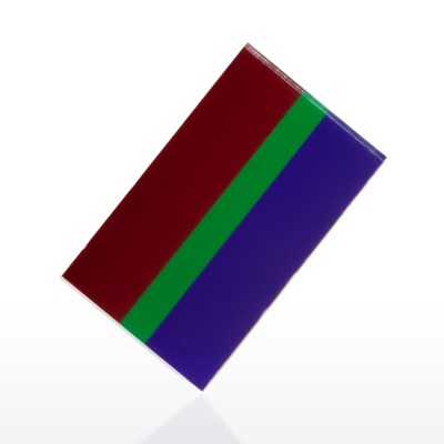
A thin film patterned optic can be applied to any vacuum compatible optical substrate material, including optical glass, certain plastics, and ceramics to produce a variety of shapes to meet your custom optical coating requirements.
• Pattern Geometries Down to 5µm
• Multiple Pattern Stacking
• Gapless Patterns – no physical space between adjacent coatings
• Custom Patterns
• Front Surface to Back Surface Pattern Alignment to ≤ 25mm
All optical elements are thin film designed, manufactured, and tested in-house.
Click here for our Photolithography Patterned Optics datasheet
Reynard is ISO 9001:2015 certified, ITAR registered, and Cybersecurity (CMMC) compliant, providing the quality standards and compliance many industries require.
Contact us for a custom quote!
CAPABILITIES
- UV curable / dissolvable polymeric photoresist
- Front to back surface patterned alignment to ≤ 25µm
- 5µm and above geometry resolution
- Multiple pattern stacking, alignment tolerance 25µm and above
- Optical coating thickness up to 7µm
- Photoresist thicknesses up to 100µm
- Dielectric and metal coatings
- As large as 18″ in diameter
- Multi-Spectral Detector Filters
SUBSTRATE MATERIAL
- Glass
- Plastics (certain types)
- Ceramics
- Metal
APPLICATIONS
- Alignment Test & Reference Patterns
- Heated Windows
- Scope Crosshairs
- Filters: Patterned & Comparison
- Beamsplitters: Polka Dot & Wideband
- Boresights
- Scopes Reticles
- Fluorescence Imaging
- Barcodes
- Pinholes and Optical Slits
- Patterns: Resolution & QC
- Alignment Test Patterns
- Devices: Non-Imaging
- Angle Measuring
- Encoder Disks
- Environmental Sensors
- Multi-Spectral Detector Filters
- Machine Vision
- Automated Inspection
- Targets: Optical & Military
- Imaging & Color Calibration
- Hyperspectral